The BeagleLogic cape: Assembly and Testing

A day before Christmas, I was greeted by a yellow DHL packet from Hong Kong. The panels had finally arrived after 8 days – I had chosen rush (48hrs turnaround) and express shipping, and it did work out well as I received them before Christmas. The boards turned out to be nice. Not dirty at all and at a price which was reasonable to me.

Assembly

Ready for assembly
Before assembly – the board with applied solder paste and a few parts

I reflowed the board with a hot air gun. Applied solder paste with a toothpick and placed the parts with the naked eye using a pair of good quality tweezers. The passives are all 0603 size (1.5mm x 0.76mm). Since I was yet to receive the batch of BSS138 FETs I ordered, I used a BC847 NPN transistor for the build instead. Reflowing left a couple of solder bridges on the 74LVCH16T245 (now onwards referred to as ‘the 245’) buffer chip (smallest pitched part on board – 0.5mm) which I removed using a solder wick. Then soldered the pin headers manually.

Cleaned up after soldering using nail polish remover. It’s terribly inefficient, and I plan to get a bottle of concentrated isopropyl alcohol (IPA) at some point of time. Here’s the finished result:

“Smoke Test”

A colloquial reference to the first power-on of the assembled circuit. I plugged the cape into the BeagleBone Black and powered on the assembly. The LEDs lit up and the board booted. No smoke or burning smell. Woohoo, test passed, or …

Errata

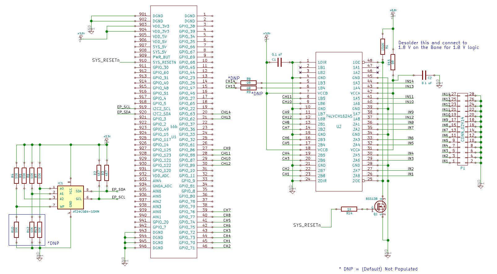
I then probed the BeagleBone P8 header pins which serve as inputs to BeagleLogic using an LED, and did the same with the input pin headers. The LED were brighter on the inputs to the ‘245 than the P8 pins, which was contrary to expectations. A quick check on the schematics and turns out that I wired the 245 to translate from rail B to rail A while connecting the inputs to rail A and the Bone pins to rail B. Whoops! However I quickly resolved the problem by lifting pads 1 and 24 (DIR1 and DIR2) off the PCB (which was simple as those were on the ends) and soldered a bit of magnet wire through and to one of the pads of C1 going to +3.3V. Neatly done, and a lesson not to design and send off PCBs to a fab while pulling an all-nighter 😛 .

Testing

Once this was done all was back on track and the circuit worked as expected. The cape as designed did not interfere with the boot-up process due to the action of the transistor pull-down that ensured that the buffer did not drive the P8 pins until SYS_RESETn signal was high.

I tested it with SPI signals upto 24 MHz using the BeagleBoard itself and results are good at a 100Msps sample rate. I could also subject the input pins to 5V freely, without fear that I would burn the board. That’s exactly what the cape is meant for, and I’m happy with the results.

I am planning to give away the surplus boards from the first batch so anyone interested in testing it out can get in touch and depending upon where you are, I may be able to send you one of the surplus unpopulated boards (no parts included) which can be assembled yourself (1 IC, 4 passives, 1 transistor and pin headers). The Cape EEPROM section can be left unpopulated without affecting the functionality.

The design files are now available here. I made some changes to the design after fixing the errata, so the cape version is bumped to 1.1 .

Suggestions and feedback on the cape are welcome. The design is Open Hardware, so you have the freedom to use it and improve it as you like. Let me know if there’s anything that could be added in the cape as there is plenty of board real estate.

Introducing: The BeagleLogic Cape

BeagleLogic Cape - 3D Render

After coding up the BeagleLogic project, I thought that it would be great to have an add-on cape for the project that provides buffering and also makes the inputs of the BeagleBone Black tolerant to TTL logic voltage levels (up to 5.5V) allowing BeagleLogic to debug external projects with ease. Hence introducing the BeagleLogic cape, the 3D render of which you can see above. The design is done in KiCad.

The design source and gerbers will be made available on the BeagleLogic GitHub repository after I physically assemble and verify the design.

Design & Layout

The cape design is simple enough to just have a single layer layout, as you can see in the render above the top layer is entirely a ground plane but for a single trace. Since the top isn’t much populated I added useful information on the top silkscreen including indexing the pin headers on the Bone on both sides.

The logic channels are accessed via 2×14 right angled pin headers. The upper row of headers are the actual logic channels while the bottom row is all GND pins. The pin headers are arranged in a MSB-to-LSB fashion. This means that the rightmost pin when viewed from the top is raw bit 0 of the captured logic samples. Note that sigrok will use the names of the actual Bone pins so bit 0 (Channel 1) is to be identified as P8_45, bit 1 (Ch2) is P8_46 and so on. The numbering is a little non-obvious but it’s because that’s the way the pins are arranged on the BeagleBone GPIO header. But don’t worry as the cape lists the pin ID of each logic channel so you don’t have to look it up in the pin diagrams.

One important point here. Only the first 12 channels can be used by default. To use the last two channels, you must disable eMMC first and solder 0R resistors or bridge the two resistors R8 and R9 on the bottom side to enable them. Otherwise the buffer will drive those two pins and you will damage the eMMC of the board and also void the warranty.

Here’s a shot of the schematic (click to enlarge). This is for reference only with respect to the current board and the released schematic may or may not be the same

Cape Schematic

The active buffer is a TI 74LVCH16T245 or equivalent. The buffer is powered from the VDD_3V3B power rail. The OE pin initially pulled is driven using an arrangment of a BSS138 N-MOSFET whose gate is connected to SYS_RESETn of the Bone. This should ensure that the logic input pins, which are also the system boot pins, are not driven by the buffer until the startup has completed.

This version of the design has a 0R resistor through which the VDD_3V3B powers the VDDA side rail of the 16245. If you remove the short and connect it to a 1.8V supply it should become compatible with 1.8V logic levels. I am however thinking of a better solution to the problem and should address this in the next released design.

There’s the officially required cape EEPROM on the bottom side as well, I presume this could be rendered redundant as the community moves towards the Universal Cape concept. But the footprints are there, just in case.

Manufacturing

The first prototype cape has been manufactured by DirtyPCBs.com as a 2-layer Black 10x10cm protopack. It has been shipped as of the time of writing and should reach me next week. I ordered the boards as a Rush order (48h turnaround time) and got it shipped via DHL so that I could have the boards in hand before Christmas rush. I would be using their services further if the boards work out well, looking forward to receive them!

Since I had left space on the panel, and there’s free panelizing so I managed to squeeze some more of my designs into the panel and make the best use of the available real estate. I would write more about those in the coming posts.

So that’s pretty much it. Design suggestions are welcome, and I’ll see if they can be accomodated in the subsequent hardware revisions. Once I test and it all works, the design files will be made available as I have written above.

BeagleLogic Week 1: Building the PRU Firmware

The first week of the Summer of code began with the build of the core PRU firmware for data capture. I coded up firmware for both the Programmable Real-Time units operating in tandem to sample the pins and transfer it to the DDR memory directly. The code can be viewed at these links:
PRU0 assembly code
PRU1 assembly code

It makes good use of the XIN/XOUT broadside interface available for inter-PRU communication allowing movement a chunk of sampled data from PRU1 to PRU0 [currently 8 registers = 16 samples = 32 bytes] in one clock cycle. PRU0 then writes the data into the DDR memory in bursts of 32 bytes. Inter-PRU signalling is achieved through interrupts.

For buffer overflow/underflow detection, there is a global byte counter running in PRU0, which is moved alongwith the logic data “for free” via XOUT. PRU0 compares the received value of the counter with the value received from the previous interrupt, and if they differ by more than 32, then there has been an overflow. Also, when the ARM core is signalled for data, an interrupt counter is incremented. The counter is compared to its previous value, and the delta here again enables us to determine if an underflow has occurred.

This approach works fine for one-shot sampling, and I have been able to achieve all the way up to 4 MSamples of 12 pins running at 100 MHz [40ms], although the limitation on the maximum sample rate is likely to be the hardware of the BeagleBone Black in this case, remember there’s a 47pF capacitive load on the HDMI shared pins, and it is yet to be tested with actual hardware.

Currently there’s only 8 MB of memory shared with the PRU for storing samples, there’s an issue with the UIO kernel driver that prevents reserving more memory. The UIO driver will not be fixed, rather the issue will be addressed in the remoteproc interface of the PRU with the kernel. Until then, there is a workaround by adding mem=448m to the boot command line in uEnv.txt, to reserve the upper 64 MB of the memory for the PRU.

Reducing the sample rate is just inserting more NOPs into the sample loop to adjust the cycles. However, availability of more room between two sampling instructions turn out to be potential cycles for performing RLE (which will be implemented very soon), which seems achievable at 50 MHz.

Overwriting previous chunks of data works fine as well, stress tested upto overwrite 500x. See here for an example run.

The amount of samples collected is still limited by only the amount of memory available. The PRUs are quite fast and capable of sample rates like 100 MHz. The only bottleneck is to hold the data and process it before it runs out, and this is the target for the coming week.

The current test code will be adapted to the sigrok bindings once it is in good shape. The current stable code is available at the repo here, and the latest development is in the “prutest” branch here

Next update due on June 4th.

BeagleLogic Update 0 – 18th May 2014

The introduction video to BeagleLogic is now released! Check it out here:

The slides are available here.

This week I spent time understanding the remoteproc implementation and UIO implementations of the kernel drivers of the PRU in the kernel source tree.

One of the important decisions this week was the confirmation of UIO implementation for the PRU drivers. Although a remoteproc implementation is a better approach, the initial implementation of the core would be in UIO, and as the remoteproc infrastructure improves, BeagleLogic will eventually migrate. Since this would be a core change, it would have minimal impact on the functionality.

All set for May 19th when the coding period commences.

Next update coming up on 21st May.